



Overview
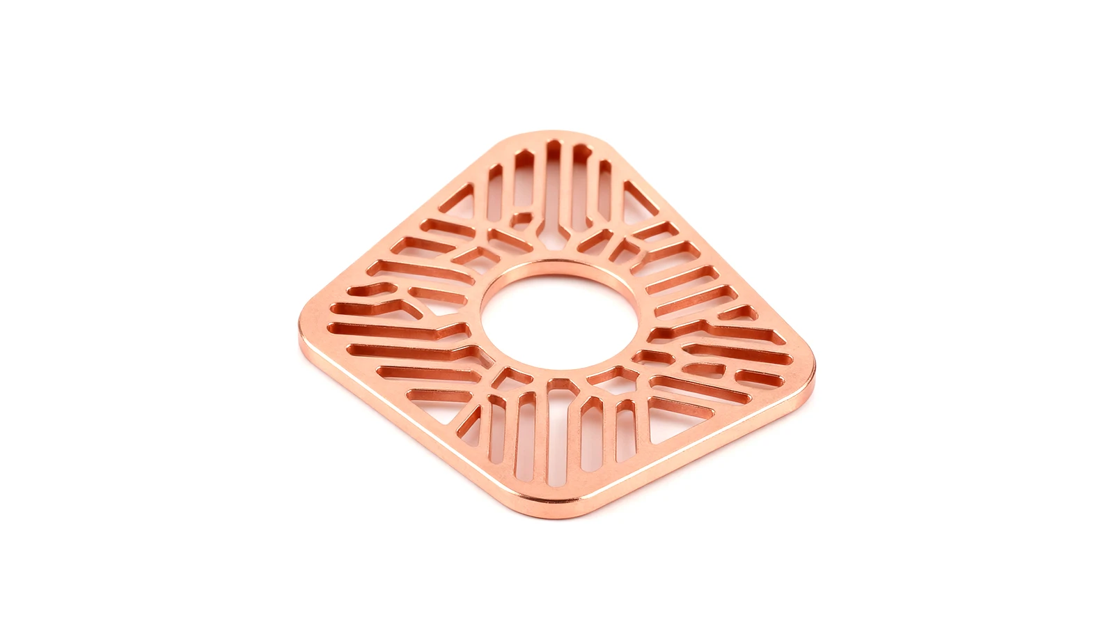
The NEWLIFE Tungsten Copper (W–Cu) IC Packaging Series is developed specifically for power semiconductor chips, RF amplifiers, microwave modules, and hermetic device carriers that require extremely stable thermal and mechanical performance. Unlike conventional copper plates or composite laminations, W–Cu materials manufactured using NEWLIFE's high-precision PM/MIM platform provide a combination of heat-spreading capability, structural rigidity, and CTE tunability that is essential for modern high-density IC architectures.
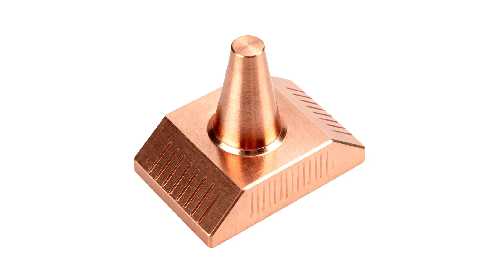
These substrates work as both a thermal interface and a structural foundation. Their tungsten phase provides low deformation and a controllable expansion coefficient, while the copper phase ensures efficient heat dissipation from active chips. Device reliability increases significantly when CTE is closely matched to Si, SiC, GaN, or GaAs; this minimizes stress accumulation around solder joints and bond interfaces, especially in high-temperature cycling conditions. NEWLIFE's material team adjusts powder ratios and sintering parameters to deliver precise CTE ranges, allowing designers to select a substrate optimized for their specific die material.
Manufacturing Technology
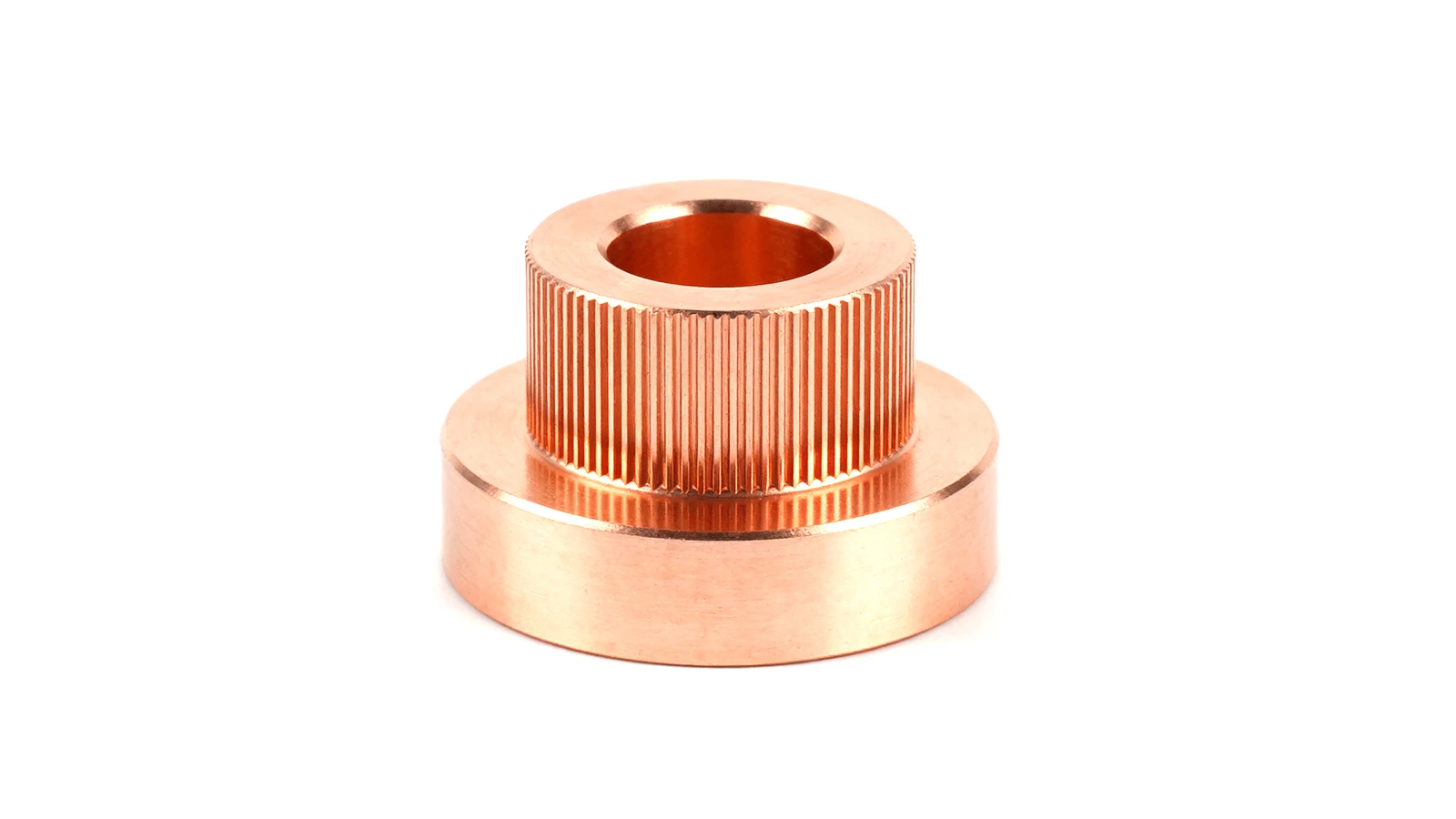
The W–Cu IC packaging parts are formed using a combination of high-pressure pressing, advanced MIM shaping, and precision sintering. These processes allow the construction of features that traditional machining cannot achieve economically, such as micro-channels for directed heat flow, stepped regions for multi-die integration, or cavity structures for hermetic component alignment. Because most dimensional accuracy is achieved at the molding stage, post-machining is minimal, making the components suitable for large-volume, cost-sensitive semiconductor production.
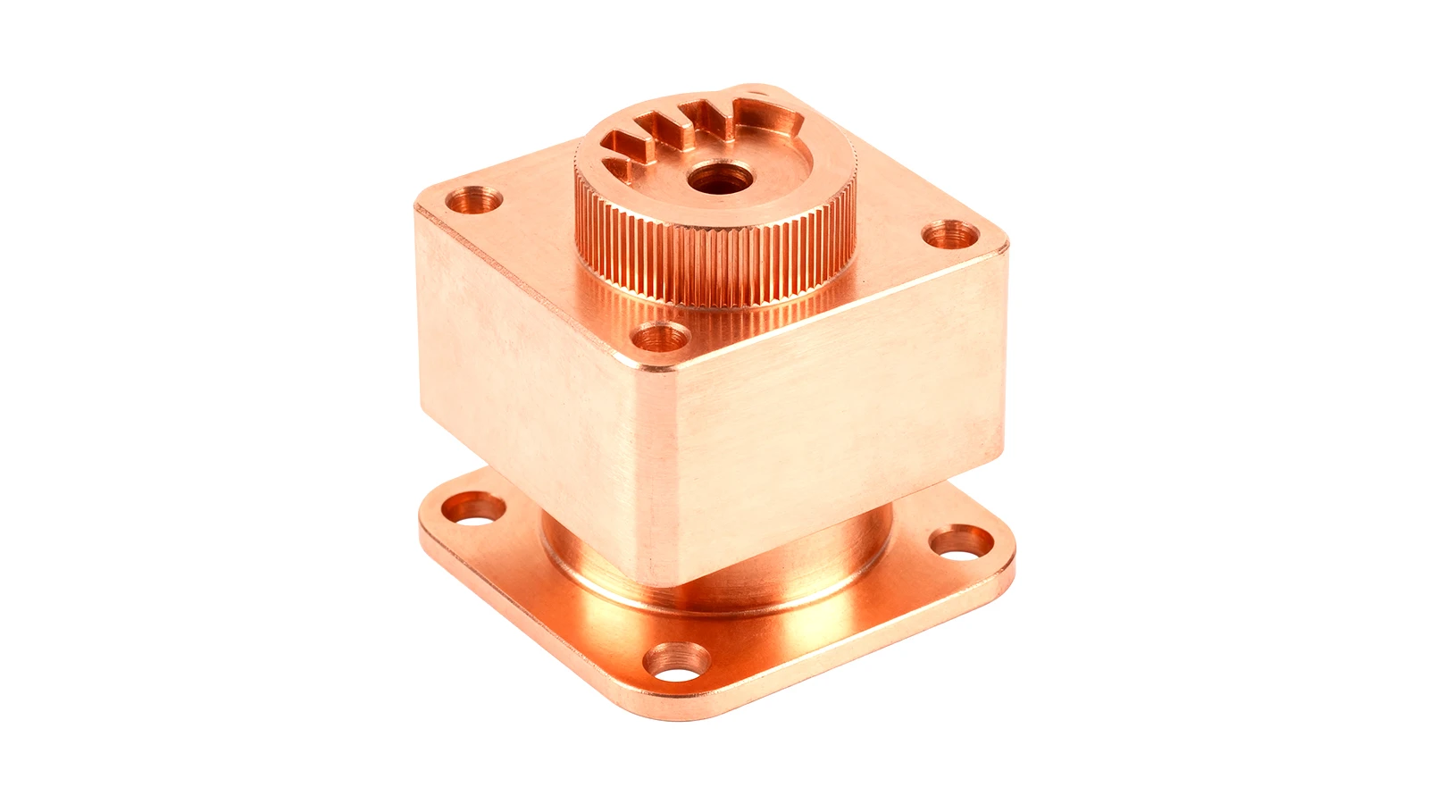
Microstructural uniformity is a core advantage. The powder metallurgy process produces tightly bonded tungsten frameworks filled with uniformly distributed copper, eliminating the inconsistent density or voids common in cast composites. This results in stronger joint integrity, reduced warpage, and predictable thermal expansion throughout the substrate.
Performance Benefits
Devices packaged with NEWLIFE W–Cu substrates experience:
- Enhanced thermal reliability due to high copper-phase conductivity
- Strong mechanical support under continuous thermal cycling
- Reduced thermal resistance between die and heat sink
- Stable electrical performance in RF and microwave modules
- Excellent compatibility with common metallization such as Ni/Au, Ag, Cu, or ENEPIG
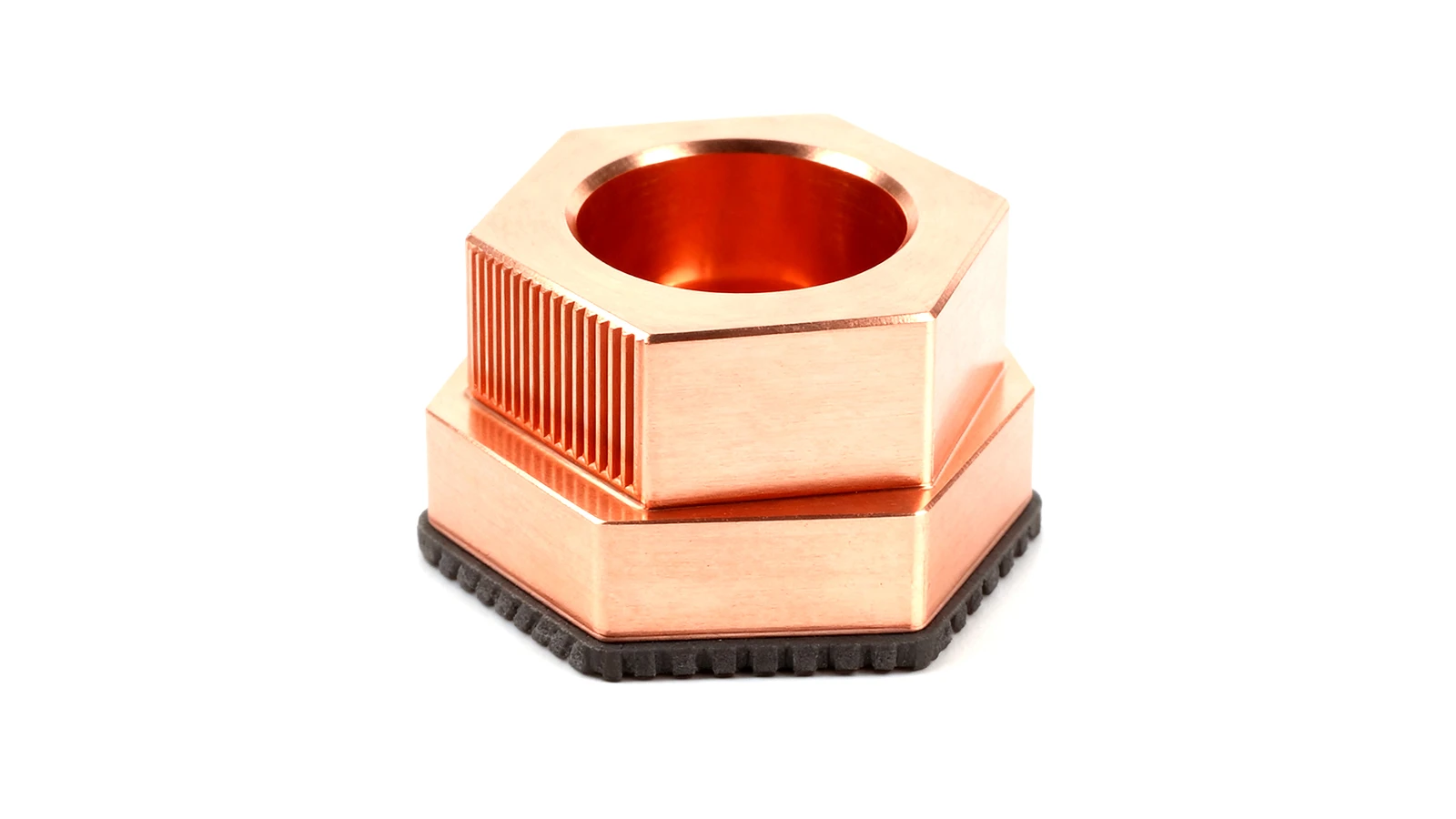
The material's high density ensures dimensional stability, which is critical for tight-tolerance IC assemblies and automated die-attach processes.
Application Scenarios
These packaging substrates are integrated into:
- High-power switching devices used in industrial power systems
- RF transistor carriers for wireless base station components
- Defense-grade hermetic microwave modules
- High-temperature SiC and GaN power stages
- Precision hybrid circuits and sealed microelectronic packages
The NEWLIFE W–Cu IC Packaging Series provides designers with a highly reliable, thermally efficient, and cost-effective substrate engineered for next-generation semiconductor modules.
Hot Tags: tungsten copper ic packaging, China tungsten copper ic packaging manufacturers, suppliers, Tungsten Copper IC Packaging, Tungsten Copper Substrate, EML DFB Thermal Component, copper thermal packaging components, Laser Diode Heat Sink, High Power Heat Sink


